Mechanism for electromechanical response enhancement and unusual thickness scaling in antiferroelectric PbZrO3 thin films. credit: Natural materials (2024). DOI: 10.1038/s41563-024-01907-y
× near
Mechanism for electromechanical response enhancement and unusual thickness scaling in antiferroelectric PbZrO3 thin films. credit: Natural materials (2024). DOI: 10.1038/s41563-024-01907-y
Lighting a gas grill, receiving an ultrasound, using an ultrasonic toothbrush – these actions involve the use of materials that can convert electrical voltage into shape change and vice versa.
Known as piezoelectricity, the ability to trade between mechanical stress and electrical charge could be widely used in capacitors, actuators, transducers and sensors such as accelerometers and gyroscopes for next-generation electronics. However, integrating these materials into miniaturized systems is difficult due to the tendency of electromechanically active materials—at the submicron scale, when the thickness is only a few millionths of an inch—to be “squeezed” by the material to which they are attached, greatly reducing their performance. .
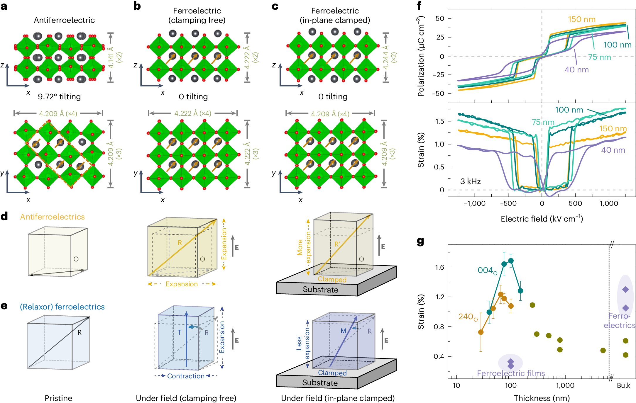
Researchers at Rice University and collaborators at the University of California, Berkeley have found that a class of electromechanically active materials called antiferroelectrics may hold the key to overcoming performance limitations due to clamping in miniaturized electromechanical systems.
A new study published in Natural materials reported that a model antiferroelectric system, lead zirconate (PbZrO3), produces an electromechanical response that can be up to five times that of conventional piezoelectric materials even in films as thin as 100 nanometers (or 4 millionths of an inch).
“We’ve been using piezoelectric materials for decades,” said Lane Martin, the Rice materials scientist who is the study’s corresponding author. “Recently, there’s been a strong motivation to further integrate these materials into new kinds of devices that are very small — like you’d want to do, say, with a microchip that goes into your phone or computer.” The problem is that these materials are usually just less usable at these small scales.”
According to current industry standards, a material is considered to have very good electromechanical properties if it can undergo a 1% change in shape or strain in response to an electric field. For an object that is 100 inches long, for example, lengthening or shortening by 1 inch represents 1% strain.
“From a materials science perspective, this is a significant answer because most solid materials can only be changed by a fraction of a percent,” said Martin, the Robert A. Welch Professor of Materials Science and Nanoengineering and director of the Rice Advanced Institute of Materials.
When conventional piezoelectric materials are scaled down to sub-micrometer (1000 nanometers) size systems, their performance typically degrades significantly due to substrate interference, which reduces their ability to change shape in response to an electric field or, conversely, to generate stress in response to a change in shape.
According to Martin, if the electromechanical performance is rated on a scale of 1-10—where 1 is the lowest performance and 10 is the industry standard of 1% strain—then clamping would typically be expected to reduce the electromechanical response of conventional piezoelectrics from 10 to the 1 range. -4.
“To understand how clamping affects movement, first imagine you’re in the middle seat of an airplane with no one on either side of you – you’ll be free to adjust your position if you get uncomfortable, overheat, etc.” Martin said. “Now imagine the same scenario, only now you’re sitting between two huge offensive linemen from the Rice football team. You’ll be ‘squeezed’ between them so that you really can’t meaningfully adjust your position in response to a stimulus.”
The researchers wanted to understand how very thin films of antiferroelectrics—a class of materials that remained understudied until recently due to the lack of access to “model” versions of the materials and their complex structure and properties—changed their shape in response to strain, and whether they were also susceptible to compression.
First, they grew thin films of the model antiferroelectric material PbZrO3 with very careful control of material thickness, quality and orientation. They then performed a series of electrical and electromechanical measurements to quantify the responses of the thin films to an applied electrical voltage.
“We found that the response is significantly larger in thin layers of antiferroelectric material than what is achieved with similar geometries of traditional materials,” said Hao Pan, a postdoctoral fellow in Martin’s research group and lead author of the study.
Measuring shape change on such small scales was not easy. In fact, optimizing the measurement setup required so much work that the researchers documented the process in a separate publication.
“With the advanced measurement setup, we can get a resolution of two picometers — that’s about one-thousandth of a nanometer,” Pan said. “But just showing that shapeshifting happened doesn’t mean we understand what’s going on, so we had to explain it. This was one of the first studies to reveal the mechanisms behind this high performance.”
With the support of their collaborators at MIT, the researchers used a state-of-the-art transmission electron microscope to observe the shape change of the nanoscale material with atomic resolution in real time.
“In other words, we watched the electromechanical actuation as it happened, so we could see the mechanism behind the large shape changes,” Martin said. “What we found is that there is an electrical voltage-induced change in the crystal structure of the material, which is like the basic building block or single type of Lego block that the material is made of. In this case, this Lego block gets a reversible stretch with an applied electrical voltage, which gives us a large electromechanical response.”
Surprisingly, the researchers found that clamping not only did not interfere with the material’s performance, but actually improved it. Together with collaborators at Lawrence Berkeley National Laboratory and Dartmouth College, they recreated the material computationally to get another look at how the clamping affects actuation under an applied electrical voltage.
“Our results are the culmination of years of work on related materials, including the development of new techniques to study them,” Martin said. “By understanding how to make these thin materials work better, we hope to enable the development of smaller and more powerful electromechanical devices, or microelectromechanical systems (MEMS)—and even nanoelectromechanical systems (NEMS)—that use more a little energy and they can do things we never thought possible before.”
More info:
Hao Pan et al, Clamping Enables Enhanced Electromechanical Responses in Antiferroelectric Thin Films, Natural materials (2024). DOI: 10.1038/s41563-024-01907-y
Log information:
Natural materials