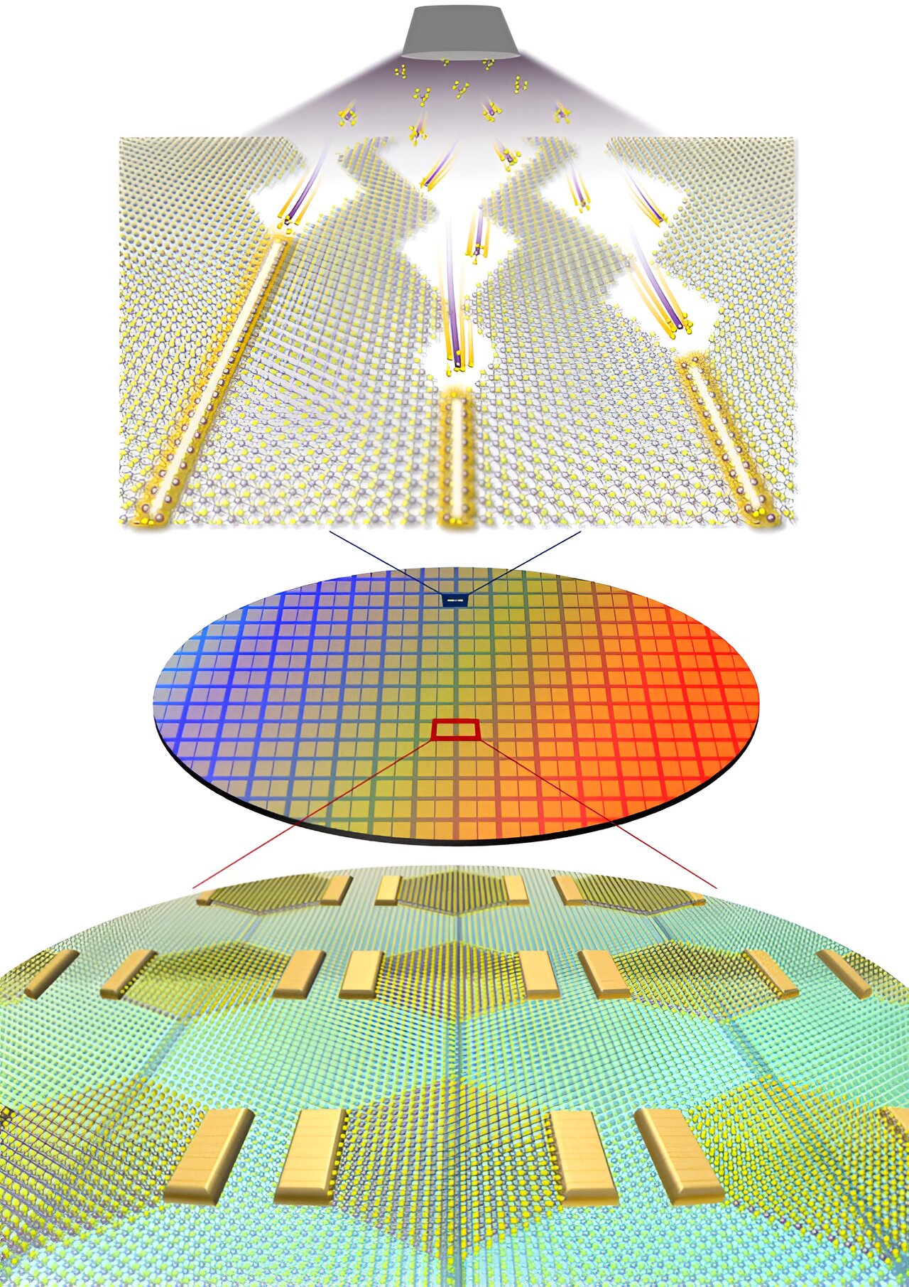
This figure depicts the synthesis of metallic 1D mirror double boundaries by van der Waals epitaxial growth (top) and a large-area 2D semiconductor integrated circuit constructed based on these boundaries (bottom). By controlling the molybdenum disulfide crystal structure at the atomic level using Van der Waals epitaxial growth, metallic 1D mirror double boundaries were freely synthesized at desired locations on a large scale. These boundaries were applied as valve electrodes to implement ultraminiaturized 2D semiconductor transistors with atomic-scale channel lengths. Credit: Institute of Basic Sciences
A research team led by Director Jo Moon-Ho from the Van der Waals Center for Quantum Solids within the Institute for Basic Sciences (IBS) has applied a new method to achieve epitaxial growth of 1D metallic materials with a width of less than 1 nm. The group applied this process to develop a new structure for 2D semiconductor logic circuits. It should be noted that they used the 1D metals as the gate electrode of the ultraminiaturized transistor.
This research appears in Natural nanotechnologies.
Integrated devices based on two-dimensional (2D) semiconductors, which exhibit excellent properties even at the extreme limit of material thickness down to the atomic scale, are a major focus of fundamental and applied research worldwide. However, realizing such ultra-miniaturized transistor devices that can control the movement of electrons within a few nanometers, let alone developing the manufacturing process for these integrated circuits, has been met with significant technical challenges.
The degree of integration in semiconductor devices is determined by the width and control efficiency of the gate electrode, which controls the flow of electrons in the transistor. In conventional semiconductor manufacturing processes, reducing the gate length below a few nanometers is impossible due to lithography resolution limitations.
To solve this technical problem, the research team used the fact that the specular double boundary (MTB) of molybdenum disulfide (MoS2), a 2D semiconductor, is a 1D metal only 0.4 nm wide. They used this as a gate electrode to overcome the limitations of the lithography process.
, a schematic of the ultraminiaturized transistor and inverter devices that make up the circuit (center), and the performance evaluation of these devices (right). ). The 1D mirror double boundary process developed by the research team was not limited to the miniaturization of individual devices, but was successfully used to construct large-area highly integrated electronic circuits. Credit: Institute of Basic Sciences")
This figure shows an optical microscope image of the integrated circuit based on 1D mirror double boundary gates (left), a schematic of the ultraminiaturized transistor and inverter devices that make up the circuit (center), and the performance evaluation of these devices (right). ). The 1D mirror double boundary process developed by the research team was not limited to the miniaturization of individual devices, but was successfully used to construct large-area highly integrated electronic circuits. Credit: Institute of Basic Sciences
In this study, the 1D MTB metal phase was achieved by controlling the crystal structure of the existing 2D semiconductor at the atomic level, transforming it into a 1D MTB. This represents a significant breakthrough not only for next-generation semiconductor technology, but also for fundamental materials science, as it demonstrates the large-area synthesis of new material phases through artificial control of crystal structures.
The International Roadmap for Devices and Systems (IRDS) by IEEE predicts that semiconductor node technology will reach about 0.5 nm by 2037, with a transistor gate length of 12 nm. The research team demonstrated that the channel width modulated by the electric field applied by the 1D MTB gate can be as small as 3.9 nm, significantly exceeding the futuristic prediction.
The 1D MTB-based transistor developed by the research team also offers advantages in circuit performance. Technologies such as FinFET or Gate-All-Around, adopted to miniaturize silicon semiconductor devices, suffer from parasitic capacitance due to their complex device structures, leading to instability in highly integrated circuits. In contrast, the 1D MTB-based transistor can minimize parasitic capacitance due to its simple structure and extremely narrow gate width.
Director Jo Moon-Ho commented, “The 1D metal phase achieved by epitaxial growth is a new material process that can be applied to ultra-miniaturized semiconductor processes. It is expected to become a key technology for the development of various low-power, high-efficiency electronic devices in the future.”
More info:
Integrated 1D epitaxial mirror double boundaries for ultra-scaled 2D MoS2 field-effect transistors, Natural nanotechnologies (2024). DOI: 10.1038/s41565-024-01706-1
Courtesy of the Institute of Basic Sciences
Quote: Scientists discover way to ‘grow’ sub-nanometer-sized transistors (2024, July 3) Retrieved July 3, 2024, from https://phys.org/news/2024-07-scientists-nanometer-sized- transistors.html
This document is subject to copyright. Except for any fair dealing for the purposes of private study or research, no part may be reproduced without written permission. The content is provided for informational purposes only.