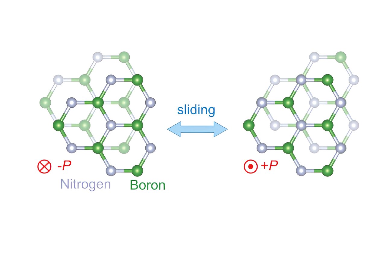
Caption: Schematic showing the crystal structure of boron nitride, the key to a new ferroelectric material that researchers and colleagues at MIT have used to build a transistor with superior properties. The schematic shows how the structure can change when two ultrathin layers of boron nitride slide past each other when an electric field is applied. P stands for polarization or negative/positive charge. Credit: Ashoori and Jarillo-Herrero Laboratories
In 2021, a team led by MIT physicists reported the creation of a new ultrathin ferroelectric material, or one in which positive and negative charges are separated into different layers. At the time, they noted the material’s potential for applications in computer memory and more. Now the same core team and colleagues – including two from the neighboring lab – have built a transistor with this material and shown that its properties are so useful that it could change the world of electronics.
Although the team’s results are based on a single transistor in the lab, “in several aspects its properties already meet or exceed industry standards” for ferroelectric transistors produced today, said Pablo Jarrillo-Herrero, the Cecil and Ida Green Professor of Physics, who led working with physics professor Raymond Ashory. Both are affiliated with the Materials Research Laboratory.
“In my lab, we mainly do fundamental physics. This is one of the first and perhaps the most dramatic examples of how basic science has led to something that can have a big impact on applications,” says Jarillo-Herrero.
Ashori says, “When I think about my entire career in physics, this is the work that I think 10 to 20 years from now could change the world.”
Among the superior properties of the new transistor:
- It can switch between positive and negative charges—essentially the ones and zeros of digital information—at very high speeds, on nanosecond time scales. (A nanosecond is one billionth of a second.)
- This is extremely difficult. After 100 billion switches, it still works with no signs of deterioration.
- The material behind the magic is only billionths of a meter thick, one of the thinnest of its kind in the world. This, in turn, could allow for much denser storage of computer memory. It can also lead to much more energy-efficient transistors because the voltage required to switch scales with material thickness. (Ultra-thin equals ultra-low voltages.)
The work is published in a recent issue of Science. The paper’s first co-authors are Kenji Yasuda, now an assistant professor at Cornell University, and Evan Zalis-Geller, now at Atom Computing. Additional authors are Xirui Wang, a physics graduate student at MIT; Daniel Bennett and Efthimios Kaxiras of Harvard University; Suraj S. Cheema, assistant professor in MIT’s Department of Electrical Engineering and Computer Science and an affiliate of the Electronics Research Laboratory; and Kenji Watanabe and Takashi Taniguchi of the National Institute of Materials Science in Japan.
What did they do?
In a ferroelectric material, the positive and negative charges spontaneously point to different sides or poles. When an external electric field is applied, these charges switch sides, reversing the polarization. Polarization switching can be used to encode digital information and that information will be non-volatile or time-stable. It will not change unless an electric field is applied. For a ferroelectric to have widespread application in electronics, all of this must occur at room temperature.
The new ferroelectric material reported in Science in 2021 is based on atomically thin sheets of boron nitride that are stacked parallel to each other, a configuration that does not exist in nature. In bulk boron nitride, the individual boron nitride layers are instead rotated 180 degrees.
It turns out that when an electric field is applied to this parallel-stacked configuration, one layer of the new boron nitride material slides over the other, slightly changing the positions of the boron and nitrogen atoms. For example, imagine that each of your hands is made up of only one layer of cells. The new phenomenon is similar to pressing the hands together, then gently moving them over each other.
“So the miracle is that by sliding the two layers by a few angstroms, you end up with radically different electronics,” says Ashori. The diameter of an atom is about 1 angstrom.
Another miracle: “nothing wears out when sliding,” Ashori continues. This is why the new transistor can be switched 100 billion times without degradation. Compare this to the memory in a flash drive made of conventional materials. “Every time you write and erase flash memory, you get some degradation,” says Ashori. “Over time it wears out, which means you have to use some very complex propagation methods where you read and write to the chip.” The new material could make those steps obsolete.
A joint effort
Yasuda, co-author of the present Science paper, applauds the collaboration involved in the work. Among them “we [Jarillo-Herrero’s team] did the material with Ray as well [Ashoori] and [co-first author] Evan [Zalys-Geller], we measured its characteristics in detail. That was very exciting.” Says Ashori, “many of the techniques in my lab naturally apply to the work being done in the lab next door. Was a lot of fun”.
Ashori notes that “there’s a lot of interesting physics behind it” that could be explored. For example, “if you think about the two layers sliding past each other, where does that sliding begin?” Also, says Yasuda, could ferroelectricity be triggered by something other than electricity, such as an optical pulse? And is there a fundamental limit to the number of switches a material can make?
Challenges remain. For example, the current way of producing new ferroelectrics is difficult and not conducive to mass production. “We made one transistor as a demonstration. If people could grow these materials at wafer scale, we could create many, many more,” says Yasuda. He notes that various groups are already working towards this goal.
Ashori concludes: “There are several problems. But if you allow them, this material fits in so many ways into potential future electronics. It’s very exciting.”
More info:
Kenji Yasuda et al., Ultrafast High Endurance Memory Based on Sliding Ferroelectrics, Science (2024). DOI: 10.1126/science.adp3575
Courtesy of MIT
This story is republished courtesy of MIT News (web.mit.edu/newsoffice/), a popular site that covers news about MIT research, innovation and teaching.
Quote: New transistor’s superior properties may have wide applications in electronics (2024, July 29), Retrieved July 30, 2024, from https://techxplore.com/news/2024-07-transistor-superlative-properties- broad-electronics.html
This document is subject to copyright. Except for any fair dealing for the purposes of private study or research, no part may be reproduced without written permission. The content is provided for informational purposes only.